This section suggested the typical design flow for task 1 based on past experience.
We aim to provide a brief guide for you to kick start. There are no right or wrong approaches, (but could be poor approaches). The minor details are up to you to decide.
A. Theoretical Calculation
Based on the design specifications assigned to your team, decide what's the ideal range of the cutoff frequency.
You should keep in mind that there's no way to suppress the noise signal that it's completely gone, our task is to suppress it enough that the wanted signal can be received successfully.
A good way to determine the minimum interference level is to vary the amplitude of the noise signal, (e.g., 1/3, 1/10, 1/20/, 1/50... of the full interference amplitude), record the received signal with AD2 at different interference levels, pass them to the Opamp_file and observe the resulted PSR. Choose a proper interference amplitude based on PSR, and calculate the desired filter suppression with the equation: 20log(targer_interference_amp/full_interference_amp). The result can be used as a reference for stopband attenuation.
Aim to achieve this level of suppression first when building the circuit, and you can improve the PSR value if time is luxurious.
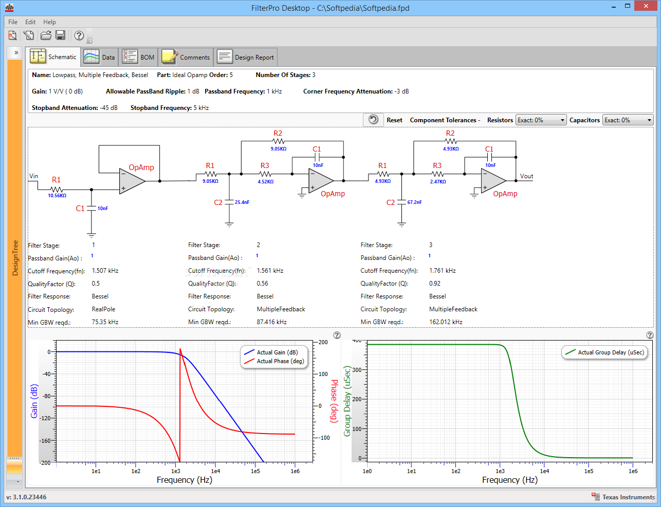
B. Theoretical Design
Based on the result from A, make use of FilterPro and generate your 1st theoretical Design.
Things you should spend time figuring out:
- How many orders/stages?
- Which response type to follow? What are the pros and cons?
- Do the provided OpAmps meet the Min. GBW requirements? If not, what to do? (Refer to Lab 3)
Note: The Min. GBW requirement could be insanely large, this should hint to you that this is an ideal design that serves as a reference, our goal is NOT to duplicate it on the breadboard.
C.1. LTSpice Simulation (Frequency Response)
Implement the design generated in B with LTSpice.
Helpful guides for LTSpice can be found here]] ></ac:plain-text-link-body></ac:link></u>.</span></p><p style="margin-left: 40.0px;"><span style="letter-spacing: 0.0px;"><ac:image ac:height="150"><ri:attachment ri:filename="image2022-1-3_17-37-56.png" /></ac:image><ac:image ac:height="150"><ri:attachment ri:filename="image2022-1-3_18-7-33.png" /></ac:image></span></p><p style="margin-left: 40.0px;"><span style="letter-spacing: 0.0px;">Run AC simulation and plot the <strong>Bode Plot of the output from each stage</strong>, cross-check the measured cutoff frequency with the designed cutoff frequency from B. </span></p><p style="margin-left: 40.0px;"><span style="letter-spacing: 0.0px;">You may notice that the untuned filter circuit is not giving you what you expected, this is normal. This could be caused by various factors, you may put down your thoughts on this in your report. </span></p><p style="margin-left: 40.0px;"><span>Adjust R values to match the design. (Refer to Lecture Notes 3 final page for cutoff tuning)</span></p><h2>C.2. LTSpice Simulation (Waveform)</h2><p style="margin-left: 40.0px;">Follow the flowchart to record the signal received by RTL-SDR and convert it to LTSpice readable file, note that you need to run TWO python files (csv2grcf.py and bin2spice.py).</p><p style="margin-left: 40.0px;"><ac:image ac:height="250"><ri:attachment ri:filename="image2022-1-12_15-3-44.png" /></ac:image></p><p style="margin-left: 40.0px;">LTSpice provides "realistic" simulation, once you've done tuning R in C.1., perform the conversion stated above, pass the resultant "<strong>sig.dat</strong>" through the <strong>LTSpice circuit</strong>, observe and save the output waveform as "<strong>test.dat</strong>".</p><p style="margin-left: 40.0px;"><ac:image ac:height="115"><ri:attachment ri:filename="image2022-1-3_18-14-9.png" /></ac:image></p><p style="margin-left: 40.0px;">Observe if distinguished <strong>HIGH and LOW </strong>with minimum noise spike is shown in the output waveform. (E.g., the blue waveform in the above figure)</p><p style="margin-left: 40.0px;">If no, repeat C.1. or consider redesigning from section B.</p><p style="margin-left: 40.0px;">If yes, pass the output waveform from LTSpice to <strong>GNURadio</strong>, "test.dat" serves as the input of "<strong>opamp_file.grc</strong>". Run and observe the PSR count.</p><p style="margin-left: 40.0px;"><ac:image><ri:attachment ri:filename="image2022-1-3_18-20-56.png" /></ac:image></p><p style="margin-left: 40.0px;">If you are satisfied with the PSR count of 1000 packets, you could move on to build the breadboard circuit now. If not, repeat C.1. or even redesign the filter. </p><h2>D. Build and Test Breadboard Circuit</h2><p style="margin-left: 40.0px;"><span style="letter-spacing: 0.0px;">Based on your result of C.2., implement the circuit physically. </span></p><p style="margin-left: 40.0px;"><span style="letter-spacing: 0.0px;"><ac:image ac:height="196"><ri:attachment ri:filename="image2022-1-3_18-23-37.png" /></ac:image></span></p><p style="margin-left: 40.0px;"><span style="letter-spacing: 0.0px;">Again, you may notice you are unable to duplicate the LTSpice design due to the restricted choice of R and Cs, this means you need to do a measurement of the cutoff and tune the Rs again to match the desired cutoff.</span></p><p style="margin-left: 40.0px;"><span style="letter-spacing: 0.0px;">Make full use of AD2 issued to you, Bode Plot, FTT, and Waveform,... there are more than enough tools for you to debug your circuit. Refer to this page to help you solve some commonly seen issues over the past semesters. </span><span style="color: rgb(255,0,0);"><strong>(Please check this page for your queries before sending emails to the teaching team)</strong><br /></span></p><p><br /></p><ac:structured-macro ac:name="tip" ac:schema-version="1" ac:macro-id="7f9d102f-8317-4a1f-8954-0711548b3d42"><ac:parameter ac:name="title">Good Practices to follow for building / testing circuits</ac:parameter><ac:rich-text-body><ul><li>Make sure your laptop is connected to a power supply, it helps provide sufficient power to your devices such as AD2.</li><li>Keep your wires neat and short.</li><li>Group the ground wires close together, as well as the power supplies.</li><li>Use capacitors to regulate positive and negative power supplies. <ac:link><ri:page ri:content-title="Common Mistakes to Avoid" /><ac:link-body><span style="color: rgb(255,0,0);">(See here for how to connect)</span></ac:link-body></ac:link></li><li>Plug in all legs/wires properly.</li><li>Trimmers (variable resistors) can be very sensitive, vibration during transportation could change their resistance. Do not press the knob with your fingers.</li></ul></ac:rich-text-body></ac:structured-macro>